 Neuerscheinungen 2015Stand: 2020-02-01 |
Schnellsuche
ISBN/Stichwort/Autor
|
Herderstraße 10
10625 Berlin
Tel.: 030 315 714 16
Fax 030 315 714 14
info@buchspektrum.de |

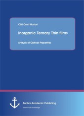
Cliff Orori Mosiori
Inorganic Ternary Thin films: Anaysis of Optical Properties
Erstauflage. 2015. 224 S. 220 mm
Verlag/Jahr: ANCHOR ACADEMIC PUBLISHING 2015
ISBN: 3-9548934-6-0 (3954893460)
Neue ISBN: 978-3-9548934-6-1 (9783954893461)
Preis und Lieferzeit: Bitte klicken
Thin films can be used to fabricate optoelectronic devices. Technology is currently focusing on ternary thin film composition because of their structure, inter-band transitions and other optical properties that can be maximized. This book discusses in detail the optical characteristics of ternary thin films and further investigates the behavior of Iron Zinc Sulphide, Lead Silver Sulphide, Copper Silver Sulphide, Copper Zinc Sulphide and Cadmium Zinc Sulphide. Thin films are of fundamental importance in modern technology.
Textprobe:
Electrical properties of CdS thin films:
Electrical properties of CdS thin films depend on the deposition condition. Evaporated films prepared for solar cell applications usually have resistivity in the range of 1 to 1000 -cm. They are usually n-type in conductivity dominated by the deviation from stoichiometry which influences the films to have S vacancies or Cd excess. Resistivity decreases as the thin film thickness increase. In thermal evaporation the [Cd]:[S] ratio during evaporation influences the electrical properties as does when doping. For CdS films doped with indium (CdS:In), the best electrical properties are obtained at a [Cd]:[S] ratio of 1:5 at which the films also exhibit resistivity values as low as 10-3 cm on CdS:In [1.5%)] samples.
Resistivity of doped evaporated films is insensitive to substrate temperature during deposition which contrasts the strong dependence of the resistivity of un-doped films on deposition temperature. CdS thin films evaporated for photovoltaic cell applications have carrier concentrations in the range 1016 to 1018 cm-3 and minority carrier diffusion lengths in the range 0.1 to 0.3 m and films grown at higher rates exhibit higher carrier concentration that increase with increase in film thickness. Those doped with indium increases their carrier concentration by almost three orders of magnitude up to a concentration of about 2% by weight and thereafter the carrier concentration does not increase. It is noted that at low indium concentrations, the carrier concentration and mobility decreases.
Chlorine has been used to dop CdS thin films. It has been reported that the CdS films doped with chlorine gas present very low photoconductivity at room temperature and their Hall mobility decreases with heat treatment. Those prepared by evaporating CdCl2 mixed CdS powders increases in resistivity and carrier concentration. A rapid incremental behaviour of mobility for the pure and low-doped films below 0.05% CdCl2 concentration was also noted. The electrical properties in spray deposited CdS films are dominated by the chemi-sorption of O2 at the grain boundaries which reduces both the carrier concentration and mobility. The films are invariably n-type with resistivity varying over a range as much as 108 -cm. Post deposition annealing in air increases the resistivity of CdS films to about 107 -cm and makes them highly photo-conducting.
A photoconductive gain from 106 to 107 with response time of about 1 ms under 50 mW cm-2 illumination has been reported. In vacuum annealing, the resistivity decreases to 1 - 10 -cm and the photoconductivity is quenched indicating the reversibility of chemisorption and desorption of oxygen. Electrical properties of CdS thin films grown by Closed-Space Vapour Transport [CSVT] show strong dependence on growth conditions especially substrate temperature. The films showed that the carrier concentration increased exponentially with increase in substrate temperature and exhibited very high mobilities while their resistivity varied from 10-3 to 1 -cm as a function of the substrate temperature. Undoped epitaxial CdS films grown by CVD exhibit resistivity between 10 and 100 -cm.
Annealing them in H2/Ar at 400 °C reduces resistivity values to between 0.01 and 0.05 -cm and when doped with indium the films possess carrier concentrations of 1018 cm-3 and Hall mobility of 65 cm2 V-1 s-1. The as-deposited sputtered CdS films exhibit a high resistivity up to 108 -cm while co-sputtering them with indium yields films with resistivity of about 1 -cm and changes their conductivity to p-type with hole mobility of 6 - 15 cm2 V-1 s-1 and a carrier concentration of about 71018 cm-3.
In most cases chemically bath deposited CdS films are n-type and have resistivity in the range 107 to 109 -cm and on annealing them in a vacuum their resistivity decreases to about 1 to 10 -cm. This reduction is attributed to desorption of O2 from the films. When annealed in air t


