 Neuerscheinungen 2011Stand: 2020-01-07 |
Schnellsuche
ISBN/Stichwort/Autor
|
Herderstraße 10
10625 Berlin
Tel.: 030 315 714 16
Fax 030 315 714 14
info@buchspektrum.de |

Jan Grabowski
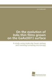
On the evolution of InAs thin films grown on the GaAs(001) surface
A study using molecular beam epitaxy and scanning tunneling microscopy
2011. 160 S. 220 mm
Verlag/Jahr: SÜDWESTDEUTSCHER VERLAG FÜR HOCHSCHULSCHRIFTEN 2011
ISBN: 3-8381-2716-1 (3838127161)
Neue ISBN: 978-3-8381-2716-3 (9783838127163)
Preis und Lieferzeit: Bitte klicken
Semiconductor nanostructures are currently of high interest for a wide variety of electronic and optoelectronic applications. A large number of such devices is based on InAs/GaAs quantum dot structures. In the present work, the pathway of the InAs wetting layer evolution is studied in detail using scanning tunneling microscopy. Thin films varying between 0.09 ML and 1.65 ML of InAs material are grown on the GaAs(001) surface in both typical growth regimes, on the GaAs-c(4x4) and the GaAs-ß2(2x4) reconstructed surface. In principle, three growth stages are found. At low InAs coverages, the indium adsorbs in agglomerations of typically eight In atoms at energetically preferable surface sites. At an InAs coverage of about 0.67 ML the initial surface transforms into a (4x3) reconstructed InGaAs monolayer. Further deposited InAs forms a second layer on top of this InGaAs ML, characterized by a typical zig-zag alignment of (2x4) reconstructed unit cells. With this second layer completed, the accumulated amount of strain induces the Stranski-Krastanow growth transition from 2D to 3D growth, and further deposited InAs accumulates in typical three-dimensional islands (quantum dots).
Dr. rer. nat. Jan Grabowski studied physics at the university TU Berlin and conducted his research in the solid state physics department investigating semiconductor nanostructures.


